In 1965, Gordon Moore made a simple observation: every year or two, the number of parts you could put on one chip, at a reasonable price, doubled. Notice what he did not say. He did not say transistors must get smaller. Smaller was just how the industry chose to deliver the doubling — and for sixty years it was the only way anyone knew. That distinction matters now, because the shrinking has gotten very hard, and everyone forgot it was only ever a means to an end.
The road that narrowed
The trouble with shrinking is money before it is physics. A leading-edge 3 nm wafer sells for about $19,500. A mature 28 nm wafer sells for about $3,000. The advanced wafer packs roughly 87× more transistors, so the math still works — if you can get in the door. But the door is the problem. The lithography machines cost hundreds of millions each. A new fab costs over twenty billion. Designing one chip costs hundreds of millions more. And the capacity is booked years ahead by a handful of giants. Transistors still get cheaper at the leading edge; they just don't get cheaper for you. A law of progress that only three companies can use isn't dead — but it isn't a law anymore. It's a subscription.
Memory already found the exit
The way out has been sitting in every SSD for a decade. Flash memory hit its own shrinking wall around 2012: the cells got too small to hold their charge. The industry's answer was not a better shrink. It was a 90-degree turn. 3D flash stacked the memory cells vertically — 24 layers in 2013, more than 300 today. Nobody misses flat flash, because bits kept getting cheaper. Just in a new direction.
Computing chips never made that turn, and the reason is heat. Making a silicon transistor takes temperatures near 1,000 °C. But the copper wiring on a finished chip is ruined above about 450 °C. So you can build one layer of transistors and wire it up — and then you are stuck. Build a second layer on top, and the heat destroys the first. That one number, 450 °C, is why computing stayed flat for the decade memory went vertical. Gluing finished chips on top of each other helps a little. But glued chips talk through solder bumps: big, coarse connections, tens of microns apart. Good enough to pass messages. Nowhere near good enough to put a memory cell directly above the transistor that reads it.
A transistor you can grow at 450 °C
This is the wall that 2D semiconductors break. These are materials — molybdenum disulfide is the workhorse — that form a working transistor in a sheet just three atoms thick. And they can be grown as a film at temperatures the wiring below survives. Our growth machine uses plasma and light, instead of heat, to drive the chemistry. So a new layer of transistors goes down on top of a finished chip like a coating, and the chip underneath never notices. Each layer is a third of a micron thick, connected downward by vertical wires as fine as the circuits themselves: millions of connections per square millimeter, where glued stacks manage thousands.
Sophon, our reference design, stacks 64 of these layers — 32 for computing, 32 for memory — on an ordinary 28 nm silicon base. The whole stack is 22.4 microns tall: less than half the thickness of a single die in an HBM memory stack. Computing can finally do what flash memory did twelve years ago.
The arithmetic of the second axis
The math is short. Shrink a transistor, and density grows with the square of the shrink. Stack layers, and density grows with the layer count — and the physics puts no ceiling on the count. The two combine into one rule: divide the process node by the square root of the layer count, and you get the chip's effective node. Sixty-four layers at 28 nm: 28 ÷ 8 = 3.5. Read that again. A process from 2011, stacked 64 high, has the same effective transistor density as the most advanced chip money can buy. On wafers that cost 6.5× less. From fabs with idle capacity. With no EUV machine anywhere in the building.
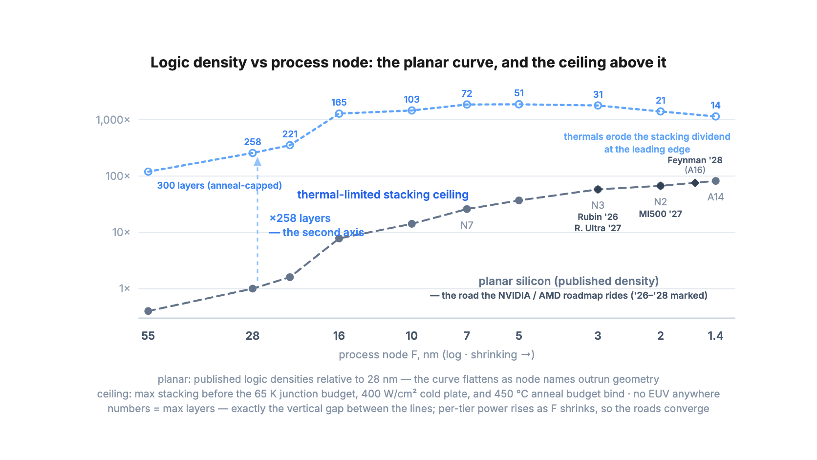
The trade works at every node, and the chart below puts both roads on one map. Read the gap between the lines: it is exactly the number of layers heat allows, and it narrows as the node shrinks, because each layer burns more power on a finer process. That gives the ceiling a peak near 5 nm — and gives the second axis its home ground on mature nodes, where the fabs are open. Our roadmap rides far below the ceiling: 64 layers today, never more than 144, and still a 1.2 nm-class effective node on a 7 nm base by 2036.
Energy tells the same story. Run at the same low voltage, an older node's arithmetic costs only about twice the energy of the leading edge's. But the layers do something shrinking never did: they put every piece of data a few hundred nanometers above the circuit that uses it. Moving data — not doing math — is what dominates AI power bills, and the vertical road simply deletes the trip. Density is what stacking promises. Proximity is what it quietly delivers.
What the vertical road is paved with
The old road was paved with lithography machines. The new one is paved with growth steps: each layer costs one deposition and one patterning pass at mature-node prices, about $52 per layer per chip. The toll is yield. Every layer you add multiplies the chip's survival odds by 99.7%, and that compounds, so stacks have a sweet spot. Too few layers, and the fixed costs dominate. Too many, and the failures do. Pure cost-per-performance favors about 24 layers; Sophon ships 64, paying an 8% premium to carry 330 GB of model memory on the chip itself. There is no free lunch here — just ordinary process engineering, with knobs and trade-offs. What there isn't is nation-state lithography.
And the vertical road carries something the old one never did. Sixty years of shrinking made computing fast while memory access stayed slow — the memory wall every chip designer fights is the old road's accumulated toll. Stacking builds the memory into the chip itself. Sophon's 32 memory layers hold 330 GB and deliver 2.10 petabytes per second inside the chip: about 100× what the best memory package on the market feeds a GPU. The reason is simple. The memory is not sitting next to the processor; it is sitting a third of a micron above it. The old road made transistors cheap and left data movement expensive. The new one makes integration cheap. And integration — not transistor count — was always the thing Moore was measuring.
Sophon's figures are modeled engineering targets from a complete published design, not measurements from shipping silicon; the whitepaper carries every equation and every risk in the open.
Moore's paper never said which direction the components had to multiply in. For sixty years there was only one direction available. Now there are two, and the second one is open to any fab built since 2011.
Frequently asked questions
- Is Moore's law dead?
- The geometric version — double density by shrinking transistors — is economically exhausted for everyone except the leading-edge few. The economic version — double what you can integrate per dollar — has a second axis: layer count. Stacking transistor layers on mature nodes continues the economic law without EUV.
- Why couldn't logic stack vertically before, when 3D NAND has shipped since 2013?
- Temperature. Silicon transistors require processing near 1,000 °C, and the copper wiring of any finished layer beneath is destroyed above roughly 450 °C. 3D flash memory sidesteps this with a specialized memory-only process that logic cannot use. 2D semiconductors grown below 450 °C are the first logic-grade transistors that can be built on top of finished, wired circuits.
- What limits how many tiers can be stacked?
- Three ceilings: yield (each layer multiplies a chip's survival odds by 99.7%, and it compounds), the total heat the bottom layer's wiring can absorb across hundreds of growth steps (roughly 300 layers), and getting the heat out of the stack. Economics bind first: the cost sweet spot at 28 nm sits near 24 layers, and the roadmap keeps stacks between 36 and 144 layers while the node shrinks underneath.